
News Archive
For updated information regarding NTNU NanoLab's activities, please go to NanoLab's homepage.
Archive

News 2020
The Rector of NTNU has allocated two PhD-positions in each of the following areas:
- biotechnology,
- nanotechnology, nanoscience and functional materials
- digital technologies (information and communication technology)
The positions will be allocated to highly innovative projects that have clear potential to contribute to NTNU’s ambition of substantially increasing the number of major national and international research grants, in particular ERC and EIC Pathfinder grants.
Scientific staff at NTNU are invited to submit research proposals by completing an online application form.
Read more about the announcement here (the link is accessible to NTNU staff only).
Application deadline January 18, 2020.
Questions regarding the announcement may be sent to vilija.balionyte-merle@ntnu.no and torbjorn.svendsen@ntnu.no. Due to festive period, please copy your inquiry to both email addresses.
Our latest feature article is out! Produced in partnership with The Chemical Engineer magazine, the report by NTNU Nano Director, John de Mello, explains how scientific instrumentation is becoming more open, more affordable and easier to make. You can view it *online* or download it as a *PDF*."
October 2020

Thor Nielsen/NTNU
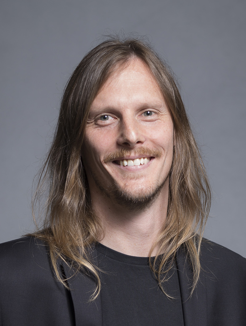
The European Research Council (ERC) provides start-up support for promising scientific projects. Through this scheme, associate professor Jan Torgersen and his collaborators have received a starting grant of 1,5 million euros for the project ELECTRODE.
The project will run for five years and address problems related to limitations on mass transport in fuel cells, using 3D printers to create porous photopolymer structures that are completely defined by a computer model.
Read more about Jan Torgersen’s research at Gemini.no
Hanna Gautun, September 2020
Living with diabetes often means having to prick your finger to test blood glucose levels several times a day.
That’s why a group of researchers in Trondheim are working on creating an “artificial pancreas” to take over this responsibility. The work is still in its early stages, but the ultimate aim is for the device to automatically measure glucose levels, and administer insulin according to the results, doing away with regular manual testing.
“We would [measure] the glucose levels every few minutes, so almost continuously,” says Karolina Milenko, a research fellow at NTNU's Department of Electronic Systems and a member of the Artificial Pancreas Trondheim research group, who is working on developing a tiny, implantable blood-glucose sensor for the device. “Then we would have an insulin pump that would be connected with the sensor, allowing the pump to administer insulin accordingly.”
Some people with diabetes already have a pump that delivers a background level of insulin automatically, which they can top up manually when they need to. And some already use a device to measure blood glucose that sits just underneath their skin. These devices, which allow for either continuous or on-demand monitoring, measure the amount of glucose in the fluid that surrounds the body’s cells, and still need calibrating with a finger prick test occasionally.
But an artificial pancreas – which won’t resemble a real pancreas in appearance, but will mimic its role – could combine these two functions, measuring glucose levels continuously and releasing insulin as needed. This would help people with diabetes to keep their blood sugar levels stable, something which is important for both short and long-term health.

In a recent paper published in Optics Letters, Milenko and her colleagues detail a sensor that could one day measure blood glucose levels. It uses two optical fibres, each 220 microns in diameter: one to send light through the test liquid to a enhancement layer, which is made of a thin gold film over a layer of nano-spheres, and second fibre to collected the signal. The sensor can identify a signature in the signal which is unique to the molecule it is designed to measure. A method called surface-enhanced Raman scattering amplifies the signal and makes it possible to see even small amounts of the molecule.
So far Milenko and her colleagues have tested the sensor by measuring the concentration of a dye, but the next step is to move on to measuring glucose itself. “Glucose is actually really difficult to measure in the levels that they are in the body, because of its very low concentration,” says Milenko. Despite the challenges, she says preliminary experiments the group have yet to publish suggest that the sensor can in fact pick up glucose.
For the next step in their research, the team are using hollow fibres, created by researchers at the University of Bath, in the sensor. The idea is that, because the hollow fibres have more favourable optical properties they should provide better sensitivity to glucose.
Milenko hopes the eventual artificial pancreas will be able to respond to changes in blood-glucose levels quicker than existing devices that go under the skin, because it will be placed in a part of the abdomen called the peritoneal cavity. “There is some research showing that the glucose levels, if you measure them in the peritoneal cavity, will have a faster response,” she says.
Continuous monitoring would also be an advantage of the device, because the on-demand testing many people use now doesn’t give them the complete picture of their blood sugar levels. “Even if you do it many times per day, you still might miss the times in a day where your glucose is too high or too low, for example, when you are sleeping, or when you're doing some activities, and you're not able to measure that specific moment,” says Milenko.
It will still be a number of years before the team has a fully functioning device – but for many people with diabetes, it will hopefully have been worth the wait.
Kelly Oakes, August 2020
We are pleased to announce that the NTNU Nano “Impact Fund” is being expanded to include funding of up to 100,000 NOK. The fund supports a wide range of activities that are likely to raise the visibility and impact of NTNU’s work in the area of nanoscience, nanotechnology and functional materials.
Applications of 20,000 NOK or less will be handled in the same way as before via a short online form, and will be considered on a competitive basis at the start of every month. We are prepared to consider any reasonable request for funding that is likely to improve the impact of nanoscience at NTNU. However, potential uses of the fund include production costs for cover articles in high-impact journals, photography or graphical artwork for publicity materials, public communication activities, the development of prototypes, and support for networking and workshops. Unfortunately, we are not able to subsidise conference attendance.
Funding requests above 20,000 NOK will be handled by a separate online form, and will be restricted to applications that aim to produce a tangible product, e.g. databases, software code and demonstrator devices. Preference will be given to ‘open’ projects that release software or hardware into the public domain on a royalty-free basis. Decisions will be made within two months of receiving the application.
Financial support from NTNU Nano should be acknowledged in any resulting publications or presentations.
(Hanna Gautun/NTNU Nano, June, 2020)

Materials science is traditionally a hands-on area of research. But Vishwesh Venkatraman, a researcher in the department of chemistry at NTNU, and his colleagues are investigating new materials from behind a computer screen.
Venkatraman got started in this area when he first came to NTNU and was working on a project to design a molecule from scratch. “You assemble the atoms and bonds and in a way that seems logically possible and at the same time synthetically feasible,” he says.
But the next step – figuring out the properties of these molecules – traditionally involves complex quantum mechanical modelling, making it extremely time-consuming. Any given molecule made up of more than 10 to 12 heavy atoms would typically need 10 to 12 hours of computer time to test, says Venkatraman. “This becomes a stumbling block,” he says. “If you have a million structures to assess, you can't actually wait for 12 hours for every computation.”
So he’s turned to data science instead. By creating a computational model using machine learning instead of quantum mechanics to predict a property of interest – whether that’s the refractive index of a polymer or the conductivity of a liquid – Venkatraman and his colleagues can cut the time needed to assess each molecule down from hours to just seconds.
Researchers can use this kind of machine learning in many different applications. In recent work, Venkatraman has investigated how dyes are affected when they’re applied to a layer of metal oxide, as happens in the manufacture of some kinds of solar cells. “When the dye is deposited on the metal oxide, it actually undergoes a change in its absorption spectrum,” he says, either shifting more towards the ultraviolet or infrared ends of the spectrum, known as a blue shift or a red shift respectively. This change affects how well the dye does its job of harvesting solar radiation, so it’s important for researchers to be able to predict what will happen after deposition.
“The challenge here was, can we predict, just from the structure of the dye, whether it’s going to have a blue shift or a red shift?” he says. He trained his model with a database of around two thousand dyes from the literature, and then used it to predict the behaviour of a further 700 experimentally-tested dyes. His machine learning model predicted that a majority would show a blue shift in agreement with experiments.
The model worked at around 80% accuracy, he says. It’s not intended to entirely replace the more laborious traditional methods of theoretically assessing materials. Instead, the idea is that you can use machine learning to narrow down the list of possibilities, and then do a more detailed analysis on the most promising candidates.
He’s also used machine learning to predict the properties of 8 million synthetically-feasible ionic liquids. Ionic liquids can be used in a variety of applications, from fuel cells to pharmaceuticals. But at the moment, finding new ones tends to require trial-and-error in the lab. By screening millions of candidates for several key properties using data-driven models, Venkatraman hopes to be able to give researchers looking for an ionic liquid with a particular melting point or viscosity, say, a head start.
One of the biggest challenges for Venkatraman and others in this emerging specialism is getting enough good data on the materials he wants to investigate. Rather than working from fundamental principles, machine learning models rely on the data they are given to come to their conclusions. “The machine learning is only as good as the data that you provide it,” he says.
But the situation is getting better, and more people are starting to adopt these methods. “There's a lot more information on materials now than even 10 years ago,” he says.
Kelly Oakes, June 2020
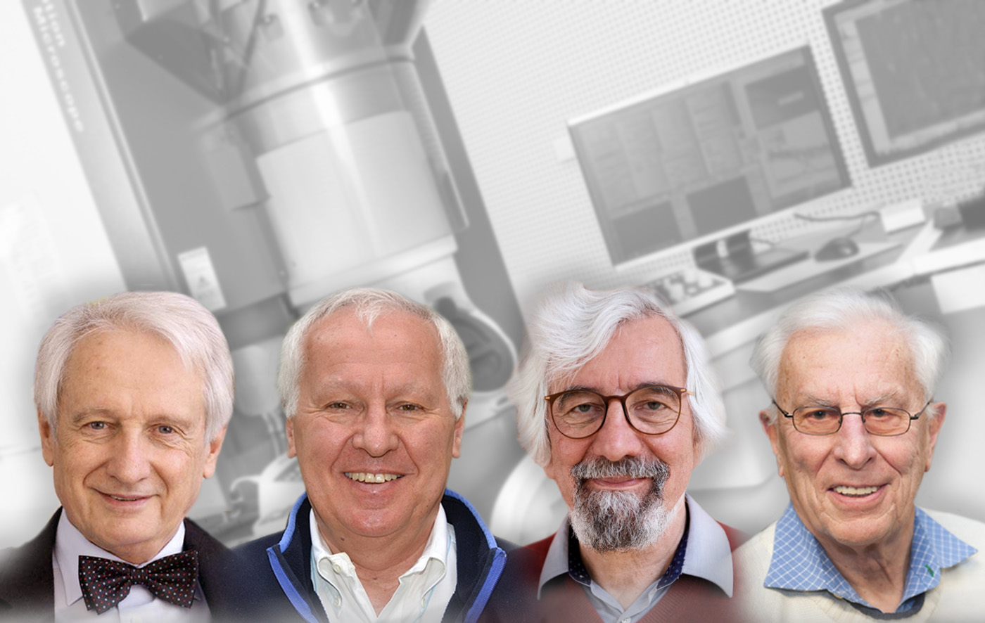
The four winners of the 2020 Kavli Prize in Nanoscience were announced yesterday as Harald Rose, Max Haider, Ondrej Krivanek and Knut Urban for "realising sub-Ångstrøm imaging and chemical analysis in transmission electron microscopy (TEM) using aberration correction." In simple terms, their work makes it possible to “see” atoms.
Due to the corona situation, the laureates will receive their medals together with the Kavli laureates in September 2022, before visiting Trondheim to give their prize lectures at NTNU.
You can read more about the Kavli Prizes, the laureates and Electron Microscopy here.
Scientific staff at NTNU are invited to submit research proposals by completing an online application form.
The European Conference on Applications of Polar Dielectrics (ECAPD) will be held at the Norwegian University of Science and Technology (NTNU) in Trondheim, Norway, from June 14th to 17th, 2020.
We are looking forward to an exciting meeting and a vivid scientific exchange and hope that you will be able to join us in June 2020.
Please forward this information to colleagues and friends, and help us spreading the news through your network to ensure that we will have an enjoyable and fruitful conference.
Deadline for abstract submission is March 15th, 2020.
We are looking forward to welcoming you in Trondheim.
The ECAPD Organizing Committee
- John De Mello
- Mari-Ann Einarsrud
- Julia Glaum
- Tor Grande
- Dennis Meier
- Sverre Selbach
- Thomas Tybell
ERC Consolidator Grants are designed to support excellent Principal Investigators at the career stage at which they may still be consolidating their own independent research team or programme. The applicant's planned research must have a ground-breaking nature, high ambitions as well as feasibility.
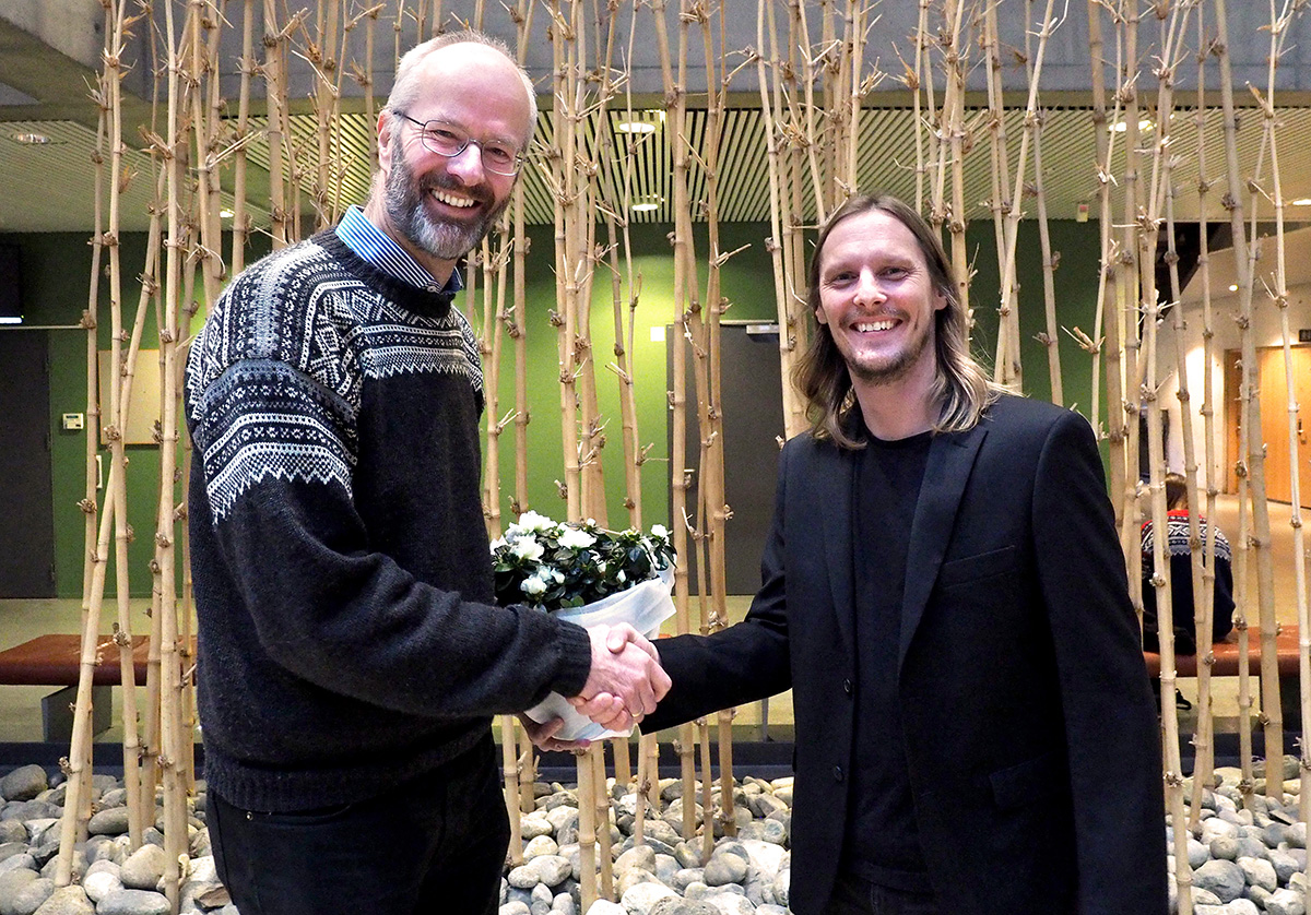
Dean Øyvind Gregersen congratulating Dennis Meier. – Receiving a grant like this is a great achievement. We look forward to see what Dennis and his research group will accomplish and how it will inspire those around them, says the Dean. Photo: Per Henning / NTNU.
The research grant amounts to just over 1,8 million euros over five years, and will be used for a project Dennis Meier calls "Atronics". The name comes from "Creating building blocks for atomic-scale electronics". The money from the EU will make it possible to add five new positions to the ten researchers who are already working with Meier
With the Atronics project, Dennis and his team will imitate the behavior and functionality of ultra-small electronic components. The research will give new knowledge in physics, and could lead to major breakthroughs in electronics. If the team succeeds, it can lead to much faster networks, and computers that barely use electricity.
Read more about Dennis Meier's research at Gemini.no
The work of Dennis and his colleagues is interdisciplinary, and is, among others a collaboration between the Department of Materials Science and Engineering collaborates the Department of Physics and the SFF Center for Quantum Spintronics (QuSpin).
(Pernille Feilberg, December, 2019)
We are pleased to announce the launch of our new “Impact Fund”, which will contribute funds of up to 20,000 NOK for activities to raise the visibility and impact of NTNU’s work in the area of nanoscience, nanotechnology and functional materials.
The scope of the Fund is not restricted, and we are prepared to consider any reasonable request for funding that is likely to improve the impact of nanoscience at NTNU. However, potential uses of the fund include production costs for cover articles in high-impact journals, photography or graphical artwork for publicity materials, public communication activities, the development of prototypes, and support for networking and workshops.
Applications should be made via a short online form and will be considered on a competitive basis at the start of every month. In exceptional circumstances, it is possible to apply for more than 20,000 NOK, but priority will be given to requests below this level. Financial support from NTNU Nano should be acknowledged in any resulting publications or presentations.
(Hanna Gautun/NTNU Nano, December, 2019)
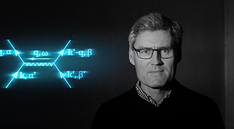
Professor Asle Sudbø at the Department of Physics has been named Fellow of the American Physical Society. Professor Sudbø is honored for his contribution in research that will contribute to the development of future information technology.
The American Physical Society (APS) is one of the world's largest organization of physicists.
The APS Fellowship Program recognizes members who have made exceptional contributions to research results in physics research, important applications in physics, management within or work in physics, or special contributions to physics education.
Professor Sudbø was nominated to be an APS Fellow "for pioneering contributions to the theory of vortex matter in highly fluctuating superconductors, super fluids and multi-component condensates".
Information technology of the future
Sudbø's research could have applications in future green information technology. This is one of the overarching research topics in the Center for Outstanding Research Quantum Spintronics (QuSpin), where Sudbø is one of four main researchers.
Sudbø is currently researching, among other things, new types of superconductors, where the connection between the electron's charge and the spin is important. In superconductors there are important conditions called vortexes, which can be viewed as a number of tornadoes (at the quantum level) of exactly the same strength.
The vortex conditions of these new materials can be manipulated by an electric field, and can provide completely new and more useful properties than before. Among other things, they could conceivably be used as qubits: elementary operating parts in quantum computers.
Prestigious award
Each year, less than half a percent of APS members are recognized by their fellow colleagues and nominated for the "Fellow of the American Physical Society".
Being named Fellow of the American Physical Society is a prestigious award, which also illustrates Sudbø's important contributions to research at the QuSpin research center, says Tor Grande, vice-dean of research at the Faculty of Science.
Pernille Feilberg / NTNU, September 2019
News 2019
ERC Consolidator Grants are designed to support excellent Principal Investigators at the career stage at which they may still be consolidating their own independent research team or programme. The applicant's planned research must have a ground-breaking nature, high ambitions as well as feasibility.
Dean Øyvind Gregersen congratulating Dennis Meier. – Receiving a grant like this is a great achievement. We look forward to see what Dennis and his research group will accomplish and how it will inspire those around them, says the Dean. Photo: Per Henning / NTNU.
The research grant amounts to just over 1,8 million euros over five years, and will be used for a project Dennis Meier calls "Atronics". The name comes from "Creating building blocks for atomic-scale electronics". The money from the EU will make it possible to add five new positions to the ten researchers who are already working with Meier
With the Atronics project, Dennis and his team will imitate the behavior and functionality of ultra-small electronic components. The research will give new knowledge in physics, and could lead to major breakthroughs in electronics. If the team succeeds, it can lead to much faster networks, and computers that barely use electricity.
Read more about Dennis Meier's research at Gemini.no
The work of Dennis and his colleagues is interdisciplinary, and is, among others a collaboration between the Department of Materials Science and Engineering collaborates the Department of Physics and the SFF Center for Quantum Spintronics (QuSpin).
(Pernille Feilberg, December, 2019)
We are pleased to announce the launch of our new “Impact Fund”, which will contribute funds of up to 20,000 NOK for activities to raise the visibility and impact of NTNU’s work in the area of nanoscience, nanotechnology and functional materials.
The scope of the Fund is not restricted, and we are prepared to consider any reasonable request for funding that is likely to improve the impact of nanoscience at NTNU. However, potential uses of the fund include production costs for cover articles in high-impact journals, photography or graphical artwork for publicity materials, public communication activities, the development of prototypes, and support for networking and workshops.
Applications should be made via a short online form and will be considered on a competitive basis at the start of every month. In exceptional circumstances, it is possible to apply for more than 20,000 NOK, but priority will be given to requests below this level. Financial support from NTNU Nano should be acknowledged in any resulting publications or presentations.
(Hanna Gautun/NTNU Nano, December, 2019)
Professor Asle Sudbø at the Department of Physics has been named Fellow of the American Physical Society. Professor Sudbø is honored for his contribution in research that will contribute to the development of future information technology.
The American Physical Society (APS) is one of the world's largest organization of physicists.
The APS Fellowship Program recognizes members who have made exceptional contributions to research results in physics research, important applications in physics, management within or work in physics, or special contributions to physics education.
Professor Sudbø was nominated to be an APS Fellow "for pioneering contributions to the theory of vortex matter in highly fluctuating superconductors, super fluids and multi-component condensates".
The program for the meeting is now available at the conference homepage:
The Norwegian NanoSymposium 2019 – Program and registration
Participation is free, but registration is required by October 1st.
The program will include talks from internationally leading scientists and early-stage researchers in many areas of science, including fundamental nanoscience, medicine, energy, and the environment. Other activities will include networking lunches, poster sessions, and a conference dinner.
We encourage master- and PhD-students, post docs and other scientists to join us these two days and learn about a whole specter of fascinating possibilities that nanoscience offers.
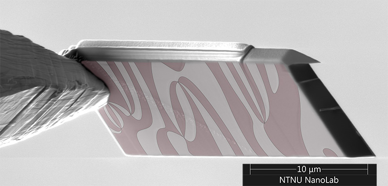
 As demand for faster and more powerful electronics grows, the size of individual components must shrink. Making these tiny components usually requires complicated techniques carried out in clean rooms with expensive equipment – but John de Mello, Bård Hoff and Sihai Luo from the department of Chemistry at NTNU are working on a decidedly lower tech approach to making what will hopefully become high performance devices.
The technique, known as adhesion lithography, involves layering two different metals onto glass, with a material to stop them sticking together sandwiched in between. Until now, finishing the process involved using adhesive tape to peel off all the extraneous materials, leaving two metals side by side separated by spaces called “nanogaps”. “A bit like pulling a plaster from your skin, it's not the most controlled process,” says de Mello.
But in a paper published in the journal Advanced Material Interfaces (see link below), the team have come up with a more controlled way to carry out this final step. Instead of peeling off the excess manually, they use a “self-peeling” layer that is applied at a high temperature – and removes itself spontaneously as it cools down.
This self-peeling layer removes some of the unreliability from the previous technique. “What we're actually doing is reducing the externally applied forces to zero,” says de Mello. “We're basically ending up in a situation where we're not disturbing the material underneath.”
The method produces components with a gap of around 10 nanometres (nm). “Below 10 nm is a target for nanogap devices,” he says, but there isn’t currently a scalable technique for reliably producing gaps this small. A smaller gap means faster electronic devices, as electrons have a shorter distance to traverse. Similarly, biosensors that detect biological molecules – for example, to diagnose disease or detect allergens in food – need gaps as small as the molecules they are designed to detect, so smaller gaps mean they can be sensitive to smaller molecules.
Being able to control the size of the gap is also key. The next step is to fine-tune the process to make devices with a range of gap widths that would be suitable for different applications. “At the moment we’re a bit like Ford – we can give you one colour, or rather we can give you one gap width, which is around this 10 nm level,” says de Mello. “What we’d like to be able to do is tailor that from gaps of two nanometres to gaps of 100 nm.”
Click here to access the paper: https://doi.org/10.1002/admi.201900243
Kelly Oakes, September 2019
NTNU's first Atomistic modelling workshop took place on Aug 16th. Two invited speakers, Prof. Trygve Helgaker from the University of Oslo and Prof. Nico van der Vegt from the Technical university of Darmstadt, presented their work on chemistry in strong magnetic fields and cosolvent effects on aqueous polymer solubility. There were 64 registered participants from NTNU from four different faculties, including several participants from the Gjøvik campus.
Thanks to sponsorship from NTNU Nano we were able to bring together researchers from all over NTNU to discuss the use of computer simulations to study a wide range of atomistic systems.
Sondre Kvalvåg Schnell, August 2019
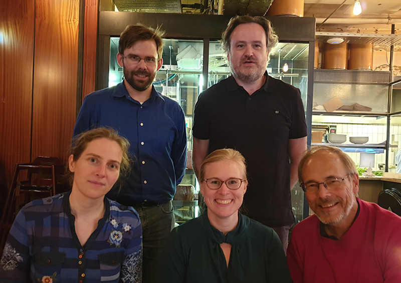
 Growing a brain in the lab might still be a far-fetched idea, but perhaps it just got one step closer.
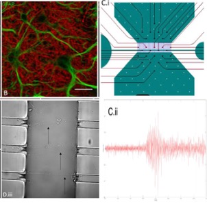
Øyvind Halaas, a professor of medicine at NTNU, in collaboration with neuroscientists Ioanna and Axel Sandvig and others, has created a mini-“brain-on-a-chip”. The biological neural network is made of just three nodes, compared to billions in a real brain, but the structure is an improvement on previous designs. Their project was part of the Cyborg initiative which aims to merge robotics and biology.
Researchers have previously tried to connect single neurons in networks, but those systems don’t always work because forming connections between individual neurons in patterns is inefficient. So Halaas and his colleagues decided to make each node a bundled group of brain cells instead.
The neurons themselves grew from stem cells, and the three nodes were connected by micro-tunnels that the neurons themselves couldn’t get through, but that did allow through their wire-like protrusions, called axons.
“The larger aim was to try to monitor the ‘thinking’ of this mini-brain-on-a-chip,” says Halaas. They used an existing commercial system to monitor the neurons’ electrical activity, and Halaas says they saw interconnection – and therefore communication – between the nodes.
The brain-on-a-chip could be used to study how brains develop and function and what exactly goes wrong when they stop working properly. “There's quite a bit of a gap from this system to trying to get neurons to form stable connections able to transmit signals, reminiscent of the thinking process in the brain,” he says. “But still, it’s kind of the beginning of a machine-learning/biology interface, which is truly fascinating.”
Brains aren’t the only organs researchers are replicating in the lab. Halaas’ other research focuses on the immune system. Though your body’s immune system isn’t a separate organ like your brain or your heart, it’s possible to recreate many of its workings using organ-on-a-chip models.
“The immune cells travel around the body, sensing their way forward towards infections or cancers, and initiating responses aimed at eliminating the threat,” says Halaas. “I've been trying to make artificial cell systems to learn how these cells communicate, develop, interact and react to stimuli.”
“The lymph node, where initiation of immune responses occurs, is particularly interesting when trying to create new solutions for vaccinations,” he added.
Ultimately, he wants to use these systems to develop cancer treatments through immunotherapy, a type of therapy that works with someone’s own body to fight off the disease. The idea would be to take cells from a cancer patient’s body and put them into the artificial immune system, before extracting the immune cells created in the artificial system and putting them back into patients.
It’s many years from being a reality, but Halaas believes it’s a promising route. “The current solutions for cancer therapy are not good enough for many patients,” he says.
This work has been carried out by Rosanne Van de Wijdeven, who worked in NTNU NanoLab on making microsystem and microelectrodes in collaboration with Ola Huse Ramstad and Ioanna Sandvig (both at Dept of Neuromedicine and Movement Science, NTNU) who did the cell work..
Kelly Oakes, September 2019
We are delighted to announce the first ever meeting of the Norwegian NanoSymposium.
Nanoscience is the hidden engine behind many of the most exciting developments in modern technology. During this two-day meeting, you will see how nanoscale materials, devices and processes are helping to solve some of mankind’s biggest challenges. The programme will include talks from internationally leading scientists and early-stage researchers in many areas of science, including fundamental nanoscience, medicine, energy, and the environment. Other activities will include networking lunches, poster sessions, and a conference dinner.
Our aim is to hold a fun, friendly and informal meeting covering all areas of nanoscience, where students and researchers from many disciplines can meet together, share ideas and make new contacts.
Thanks to sponsorship from NTNU Nano, the NanoNetwork and the Research Council of Norway, there is no participation fee, but you will need to register your attendance through the conference homepage.
Read more about the programme and registration here.
We very much look forward to welcoming you in Trondheim in October!
Imagine a bone implant that actively stimulates the recovery of the damaged tissue slowly dissolves inside your body as it’s taken over by your own bone.
This new kind of implant is not a reality – yet. But, if Julia Glaum and her colleagues have anything to do with it, it could exist one day.
Glaum, an associate professor in the Department of Materials Science and Engineering at NTNU, is figuring out how we can take advantage of the piezoelectric effect to make the next generation of biomedical implants.
Piezoelectric materials create an electric charge when you apply mechanical pressure to them. They are used in many situations, from a buzzer in your phone to the pickup on an electric guitar.
Our bones also display piezoelectric properties: If you press on a piece of bone, it creates an electric charge. “One of the theories is that bone uses these charges to know where and where not to grow, and how to heal when it’s broken,” says Glaum.
By creating implants made of piezoelectric materials, we could tell the bone where to grow. “If you could guide the bone cells to grow into the implant material, by providing these charges, you could make an implant that is stable for a longer time,” she says.
These implants would also hopefully improve the healing process, and perhaps one day even become temporary stop-gaps instead of permanent fixtures.
This is a young and relatively unexplored research area, says Glaum, so these implants are not likely to be here any time soon. But her team is making headway with the basic science needed to lay the foundations.
One unexpected finding so far is a material that dissolves under the right conditions. “Some of the materials that we make, depending on how we make them, are either very stable in liquid environment or dissolve very fast,” she says.
This wasn’t exactly what the team was looking for during the experiment in which they discovered this fast-dissolving material – but, now they’ve found it, Glaum can see the upside. They’ve since been able to make it break down over the course of a day, or keep it in one piece for “weeks and weeks”, simply by varying the way it is made.
“If you could tailor the time that it takes until it dissolves, it would just get replaced by human tissue,” she says. “That would be the ideal third-generation biomaterial.”
Kelly Oakes, June 2019)
The Nordic Nanolab Network (NNN) held its fourth Nordic Nanolab User Meeting, NNUM2019, on May 7 – 8.
NNUM is an informal meeting place for PhD-students, post docs, researchers and engineers working in the fields of nanostructuring and nanocharacterisation, and offers a wide range of technical tutorials and invited research talks on topics such as etching, thin-film technologies, lithography and characterisation. All participants have the opportunity to present their research at a poster session, with this year’s prize for the best poster going to Anders Strømberg from NTNU for his contribution: “Apparent Superpatterns in SEM Images of Small Periodic Structures”. Congratulations Anders!
The participants were also offered guided tours of DTU NanoLab as well as a spectacular dinner on Tuesday evening at the Cirkus, downtown in Copenhagen. All together 233 people attended the meeting, including 32 from NTNU. Read more about NNUM2019 here.
The next meeting, NNUM2021, will be hosted by Chalmers University in Gothenberg.
Hanna Gautun, May 2019
 If you’ve ever set foot on an icy pavement you’ll understand the importance of a good de-icer.
But ice doesn’t just get in the way of people’s daily lives. Infrastructure like aircraft, transmission cables, and offshore oil platforms can all be disrupted by ice, with potentially disastrous consequences.
That’s why Jianying He, a professor of nanomechanics at NTNU, and her colleagues are coming up with new ways to crack the problem of ice build-up.
“Nobody wants to go out in the winter to clean away ice, so we need to find a solution to avoid ice forming on the surface,” says He.
We used to think that the best way to tackle ice was to make surfaces repel water – the idea being that if water can’t build up, it can’t freeze – but it turns out that just slows down the formation of ice, and doesn’t stop it entirely.
So, He and her colleagues decided to try another tactic: they’d let the ice form, but find a way to get rid of it afterwards. The most promising method works by creating lots of cracks that make the ice break off from the surface of its own accord. It’s similar to how the perforations between postage stamps make it easier to tear them apart.
 The method – called the macro-crack initiator, or MACI – involves applying a soft layer with inner holes on top of the surface you want to protect from ice. The soft layer fluctuates as ice forms on top of it, triggering lots of small cracks. This leads to whole layers of ice shearing off from the surface under their own weight. “Ice itself is rigid,” says He. “Usually it moves like a whole piece.”
MACI is working remarkably well, she says, reducing the ice adhesion – a measure of how much the ice is stuck to the surface – even more than the team thought it would.
The next step is improving the durability of the material. Materials with lower ice adhesion are typically softer. To counter the loss in durability that comes from this softness, the group have designed a self-healing elastomer that works to fix any damage to the material.
Their coatings are not in use outside of the lab yet, but He doesn’t think it will be too long before they are. At the moment they could be used on something small, she says, say a webcam that’s exposed to the environment.
But after some more characterisation work – and some field tests – they could be coming to an oil platform or aircraft near you.
Kelly Oakes, May 2019
 A new research centre is about to give Norway a window into how its rich mineral resources can be turned into useful – and more environmentally-friendly – materials.
The Norwegian national centre for minerals and materials characterisation, known as MiMaC for short, promises to look at every step of the process of turning minerals into materials. The centre is a joint project of NTNU, the Geological Survey of Norway and research company SINTEF.
When it’s fully up and running by the end of the year, it will be made up of five world-class instruments allowing researchers to look at materials in different ways, from the atomic scale up to the microscale.
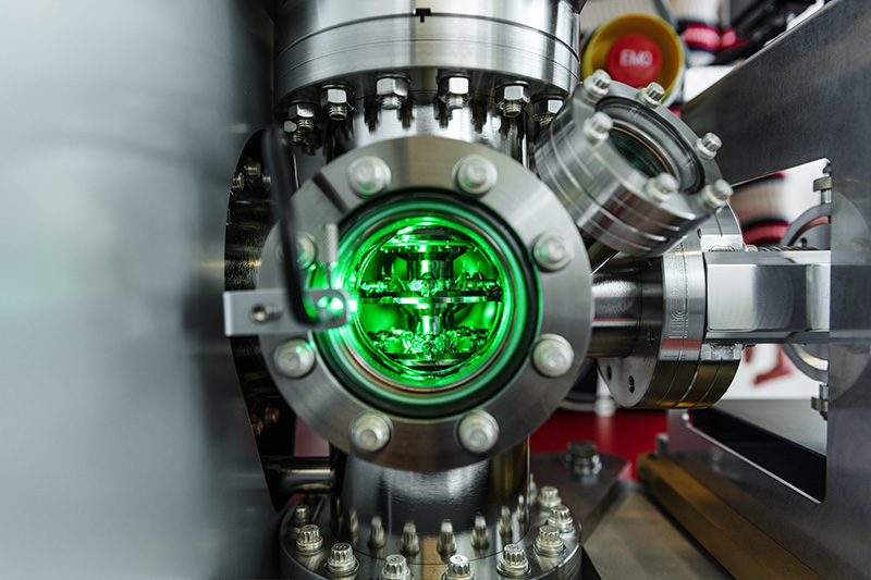
But the crown jewel of the project is already in place: a state-of-the-art atom probe that can image materials in three dimensions. It works by using laser or high voltage pulses to evaporate away the tiny sample you put into the probe, pushing its way through a few atoms at a time.
“You can reconstruct exactly where every single atom is sitting,” says Jostein Mårdalen, head of the Department of Materials Science and Engineering at NTNU. “We have a tool which is much more accurate - with higher resolution and better performance - than any other material science instrument available.”
As a national centre, MiMaC is open to scientists from other institutions who want to use its instruments. Mårdalen says he hopes that other researchers will take advantage of the atom probe to see objects such as fossils and even meteorites in a new light.
But the main reasoning behind MiMaC is more down to Earth. Using the centre’s instruments, researchers will look at the whole lifecycle of minerals: from their extraction and processing, to their design and production, and eventually their re-use or recycling.
Until now, neither research nor industry has had such a complete view, leading to inefficient ways of making materials. For example, a raw material might be stripped of impurities, only to have some new elements later added back in to make an alloy.
Now demand for greener materials is growing, Mårdalen hopes MiMaC will help both research and industry change. Seeing the full picture, he says, should allow researchers to come up with ways to make manufacturing processes less wasteful and better for the planet – for example, by finding new ways to use recycled materials. “The industry now is thinking how to be greener,” he says.
Kelly Oakes, March 2019
Read more about the instruments available through MiMaC here.
Each year the Rector sponsors a university-wide competition for two PhD positions in nanoscience, nanotechnology and functional materials, open to nano-active research groups in all faculties.
The results of this year’s competition are now out:
One position has been awarded to Jianying He and Helge Kristiansen from the Department of Structural Engineering to develop high thermal conductivity interface materials for metal/polymer interfaces; while the other has been awarded to Sverre Magnus Selbach, Mari-Ann Einarsrud and Sondre Kvalvåg Schnell from the Department of Materials Science and Engineering to develop high performance solid-state Li electrolytes for Li-ion batteries.
We wish both research teams success with their projects, and look forward to reporting on their progress in future news items.
 At the border between physics and material science, Dennis Meier and his colleagues are searching for a new kind of electronics.
They hope to make circuits that are smaller, faster, and better for the environment than today’s electronics, by taking advantage of defects that already exist within materials. The electronic components the team have made so far are just a few atoms long, and could eventually be connected together to form circuits that measure mere nanometres across – far smaller than those we use today.
“We're working at the limit of what is doable in a solid-state system when you want to construct electronic components,” says Meier, a professor in the Department of Materials Science and Engineering at NTNU.
The defects used to create these components are made when two parts of the same material have different properties. For example, their electric dipole moments – a measure of the distribution of charge in a material – might point in different directions. When these contrasting sections meet at an interface, they create what is known as a domain wall. The domain wall doesn’t behave like the rest of the material – for instance, it might be electrically conducting, even though the rest is an insulator.
 So far Meier’s team have created two electrical components using domain walls: a digital switch and a half-wave rectifier. A rectifier turns alternating current that reverses direction regularly to direct current that just flows one way. The next step in his research is to connect components together. Once that’s possible, the team can start thinking about creating logic gates and doing some basic computing with the circuits.
Theoretically, circuits made with these materials could be tweaked when new technology demands it. “Once you have made your nanoscale circuit you can update it, you can upgrade it if needed, or even erase it and rewrite it – all within the same material,” says Meier.
Because domain walls occur naturally in materials, the production process should – in theory – be simple. “The interfaces are always there and they are perfect, no additional work is needed,” says Meier.
Kelly Oakes, March 2019
 We are delighted to report the appointment of Kelly Oakes as the new science writer for NTNU Nano. Kelly is a freelance writer who specialises in science, health, environment, and technology. Her work has been published in New Scientist, BBC Future, Nature, BuzzFeed, and many other publications. She has a degree in physics and a master's in science communication from Imperial College London. Please click here for lots more information about Kelly’s extensive experience in science journalism.
Kelly has just completed her first two articles for NTNU Nano, with more on the way. If you have interesting research to report and would like it communicated to the wider scientific community in a clear and accessible way, please get in touch!
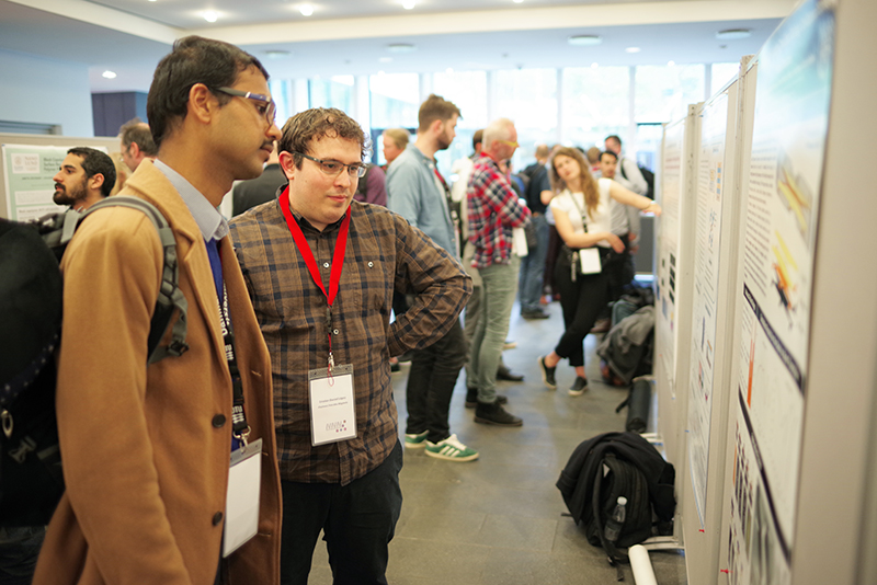
Congratulations to the master students in nanotechnology for a fun and informative set of talks at the Grey Goo Symposium on Feb 17. Some great science presented with humour and flair - learn more about what went on here.
Hanna Gautun, February 2019
You are hopefully aware that the Research Council of Norway (RCN) is changing the way it handles research proposals. The biggest change is the introduction of a common 10th April application deadline for most of its funding schemes. (Some schemes have deadlines in September, but these are mainly related to projects with industry involvement).
The RCN has introduced new portfolio boards updated its evaluation criteria (which now relate to “excellence”, “impact” and “implementation”), and introduced new templates for research proposals and investigator CVs. It has also placed some new restrictions on the number of applications that you can make as a principal investigator. You can find a helpful summary of the changes in this presentation. The following calls are likely to be the ones that are of most interest to nano-researchers: FRIPRO (basic research projects), Nano2021 (nanotechnology and advanced materials), BEDREHELSE (better health and quality of life), BEHANDLING (diagnostics, treatment and rehabilitation) and ENERGIX (energy research). However, nanoscience obviously has a valuable role to play in other programmes too, so be sure to check out all of the calls.
Unfortunately, if you are planning to resubmit an unsuccessful application from a previous funding call, then you will need to make substantial changes to its format and content to satisfy the new procedures. On the other hand, the changes do bring the RCN into closer alignment with Horizon 2020 criteria, so you will hopefully be able to use your RCN proposal as the basis for a future H2020 funding application.
Be aware that the move to a common once-per-year submission deadline means there are no “second chances” if your application is unsuccessful. You are therefore strongly advised to enlist the help of some trusted colleagues to review your proposal and suggest improvements to its structure and content; many departments are currently in the process of setting up formalised peer review procedures to assist with this.
One final warning, the common submission deadline is likely to place considerable pressure on your Department’s management and administrators, so please make sure you engage with them well in advance of the application deadline.
And remember, if you are planning to use any of the central infrastructures such as the NanoLab in your work, you will need to discuss the budget with their administrators too. Please contact the director of NTNU NanoLab, Peter Köllensperger if you need advice regarding choice of processes and budgeting.
Don’t delay – the clock is ticking!
News 2018
 We are delighted to announce the appointment of Dr. Peter Köllensperger as the new Director of NTNU Nanolab. Peter is already well known to many NanoLab users, having acted as the interim Director since August 2017. With an interesting and varied background that has spanned the academic and commercial worlds, Peter has a great understanding of the diverse needs of the Lab's academic and industrial users. After graduating from Imperial College London with a PhD in biomedical engineering, he began his professional career in investment banking at Jefferies International, specialising in the pharma, biotech and medtech sectors. He returned to Imperial to take up a Royal Academy of Engineering Enterprise Fellowship, developing nanostructured electrochemical biosensors. A Marie Curie Fellowship brought him to NTNU in 2014, and he has been closely involved with the NanoLab ever since. We wish him every success in his new(ish) role!
November was the month of our thirteenth “nano symposium”, which took place at NTNU’s

Kalvskinnet campus in central Trondheim. With well over a hundred participants from across NTNU, this two-day annual event has always been one of the best opportunities to learn about the amazing breadth of nano-related research happening at the university. This year’s meeting was no exception. The presentations covered a wealth of topics, including the synthesis of nanomaterials and nanostructured surfaces, the development of new sensor technologies, solar energy, quantum computing and many more. This year’s prize for the best oral presentation went to Anders Strømberg whose talk “Unconventional Computing with Artificial Spin Ice” described how two-dimensional lattices of interacting nanomagnets offer an efficient and highly parallel approach to computation. The prize for best poster went to Stephanie Burgmann, a first-year PhD student who impressed the judges with her firm grasp of detail. You can find a complete list of the talks and posters, including abstracts by clicking here(pdf).
In addition to the participants from NTNU, we were also fortunate to have two external speakers at the meeting, Prof. Andrew de Mello from ETH, Zurich (who spoke on the application of microfluidics to ultra-high-throughput chemistry and biology) and Dr. Wilhelm Glomm from Sintef Industry (who described how micro- and nano-encapsulation technologies can be applied to food production and healthcare). Many thanks to them both for their inspiring and well-pitched talks. And finally, a big thank you to Hanna Gautun and Berit Myhre for their immense efforts in putting together such an enjoyable and well-planned programme!
Congratulations to the winners of the 2018 Kavli Prizes. 
In the ten years since their inception, the Kavli Prizes have established themselves as some of the most important prizes in the international scientific calendar. Founded in 2008 by the Norwegian-born businessman-turned-philanthropist Fridjtof (“Fred”) Kavli, the prizes recognise exceptional breakthroughs in the fields of astrophysics, nanoscience and neuroscience. The 2018 astrophysics prize was awarded to Ewine Van Dishoeck “for contributions to observational, theoretical, and laboratory astrochemistry”; the neuroscience prize was awarded to A. James Hudspeth, Robert Fettiplace and Christine Petit “for their pioneering work on the molecular and neural mechanisms of hearing”; while the nanoscience prize was awarded to Emmanuelle Charpentier, Jennifer A. Doudna and Virginijus Šikšnys “for the invention of CRISPR-Cas9, a precise nanotool for editing DNA.”

NTNU is fortunate to play a key role in the Kavli prize celebrations, acting as the official host for the Prize Lectures in nanoscience and neuroscience. This year’s lectures were held in Trondheim on the 6th September, two days after the official prize ceremony in Oslo. During the morning we were treated to a series of inspiring lectures by the Laureates, touching on the science behind their research and the consequences for society at large. Since we are writing for NTNU Nano, it is only right that we should say a little bit more about the subject of the nanoscience prize: CRISPR-Cas9 is a gene editing tool that simplifies the removal, addition and alteration of sections of DNA from the genome, making genetic modification easier than ever before; intriguingly, the technique has its origins in an ancient mechanism that certain bacteria use to defend against viral attack. By making the process of gene editing faster, cheaper and more reliable, CRISPR-Cas 9 offers numerous opportunities for improving clinical practice; at the same time, however, the vastly increased simplicity of gene editing raises profound ethical questions that will be debated for many years to come. If you would like to learn more, you can find a clear and simple discussion of the technology here: https://www.yourgenome.org/facts/what-is-crispr-cas9.
Following the prize lectures, a terrific line-up of guest lecturers presented on wider topics in nanoscience, with Nobel-Prize laureate Albert Fert from Université Paris-Sud speaking on magnetic disturbances in thin-film magnetic materials; Chris Palmstrøm from UC Santa Barbara describing how the epitaxial combination of dissimilar materials can lead to precision-engineered structures with novel physical properties; Kristina Edström from Uppsala University describing how the selective use of nanostructurally optimized inorganic materials may allow for a new generation of safe, recyclable and high-capacity batteries; and Albert van den Berg from the University of Twente explaining how micro- and nanofabrication technologies are enabling the development of chip-based devices for chemical sensing, modeling of genetic processes, and the implementation of artificial organs. All in all, this was a fascinating and deeply inspiring day of talks from researchers at the absolute forefront of nanoscience and nanotechnology. We are already looking forward to hosting the next series of Prize Lectures in 2020!
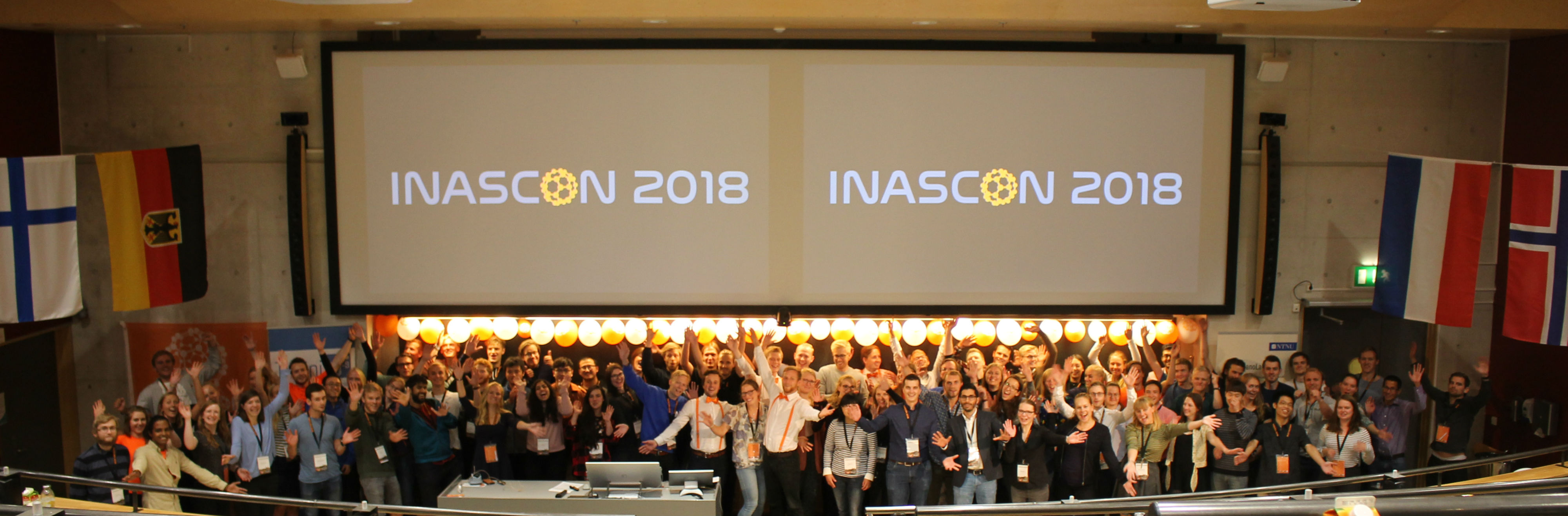
John de Mello, the new director of NTNU Nano, reports on NTNU’s hosting of the International Nanoscience Student Conference, INASCON 2018
I arrived in Trondheim in early August, which very fortunately coincided with NTNU’s hosting of the International Nanoscience Student Conference August 7-10. This student-run, three-day meeting will definitely go down as one of my personal highlights of the year. In the months running up to the meeting, I had the opportunity to watch the conference plans take shape, and I was ‘blown away’ by the professionalism and creativity of the student management team. Arranging a conference with 142 participants from across the globe is a huge undertaking; and, in this case, it was made doubly tough by the need to squeeze in all of the preparations between work assignments, research projects, and exam revision!
Through an impressive mixture of ambition and perseverance, the INASCON team put together an outstanding programme of talks and events, securing a superb line-up of world-leading experts in numerous aspects of nanotechnology (including the 2002 and 2016 Nobel chemistry laureates Kurt Wüthrich and Sir Fraser Stoddart). The diversity of talks was immense, covering self-assembly, molecular machinery, photonics, electronics, analytical science, imaging, healthcare, potential solutions to the energy crisis and many other central topics in nanoscience. Added to this were live demonstrations, panel sessions on battery technology and commercialisation, and a number of fun interactive sessions (including, a little oddly, a group rendition of “Hode, skulder, kne og tå” complete with actions).
All in all, there was a great balance of education and entertainment that kept the audience 'captivated' from beginning to end. I offer my congratulations to the whole INASCON team for putting together one of the best organised and most enjoyable conferences that I have attended in my career to date. And I wish the very best of luck to the students at Tsinghua University in Beijing, who will be hosting the next INASCON conference in July 2019.
Don’t miss it!