
Nanoelectronics, nanomagetism and nanophotonics - NTNU Nano
Nanoelectronics, nanomagetism and nanophotonics

Information- and communications technology (ICT) has experienced a tremendous growth the last 40 years. Especially, development within electronics, photonics and magnetism has lead to new, cost efficient components. A continued development of this field will, to a large extent, depend on nanotechnology.
In addition, electronic and optical properties on the nanoscale may become important for the development of new communication systems. Electromechanical systems also move towards the nano-level. By applying nanotechnology, both mass and dimensions can be reduced. This may, for example, lead to increased sensitivity of sensors for application in electronics, optics and biological systems. Studies of nano-scale magnetic structures facilitate application of the electron spin of different materials for many purposes.
Several directions of research within nanoelectronics, nanophotonics and nanomagnetism take place at NTNU. Perovskites is a class of materials with a large number of different physical properties, such as superconductivity, magneto-resistance and ferroelectricity. Several groups are engaged in this field. Photonic nanowires of GaAs for applications in eg. lasers and detectors is another field of research at NTNU, which depend to a large extent on nanotechnology.
Exampleas of our research
Improved domain-wall dynamics and magnonic torques using topological insulators
By determining the magnetization dynamics that arise when a thin-film ferromagnet is deposited on a topological insulator (TI) a number of interesting physical effects have been discovered. Read more about this here.
Controlled graphene formation on semiconductors
 In this project, a method for growth on diamond and SiC at moderate temperatures, by making use of a chemical intermediate (in this case Fe/FeSix) has been developed.
Read more about this here.
Epitaxial growth of vertical nanowires on graphene
 By utilizing the reduced contact area of nanowires, we have shown that epitaxial growth of a broad range of semiconductors on graphene can be achieved.
Read more about this here.
Staggered Dynamics in Antiferromagnets by Collective Coordinates
 The dynamics of antiferromagnets are described by equations which are very complex and with many degrees of freedom. This work presents a theory which is conceptually much simpler and which uses collective coordinates to describe staggered field dynamics in antiferromagnetic textures.
Read more about this here.
Modelling of quantum dots within semiconductor nanowires
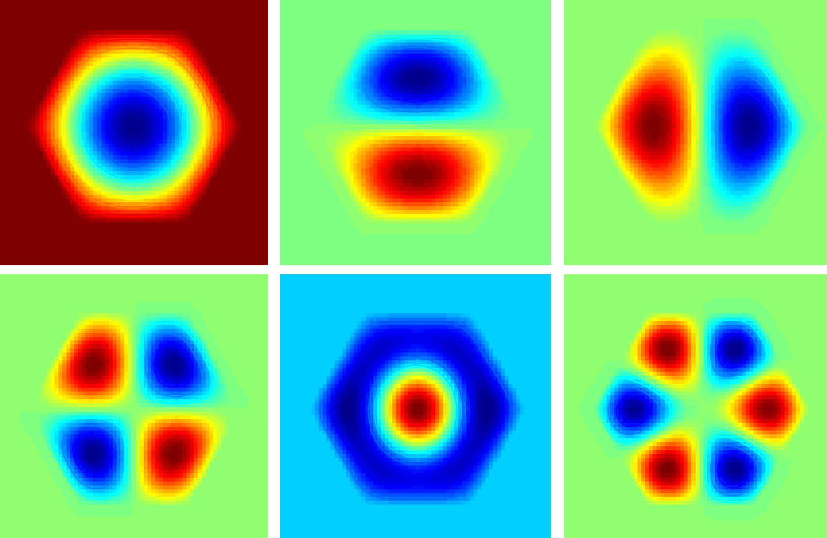 The electro-optical properties of semiconductor nanowires can be modified by growing quantum dots (QDs) within the wires. To predict the optical transition probabilities, the wavefunctions of the electrons and holes in GaAs QDs in an AlGaAs nanowire have been calculated using the k.p method.
Read more about this here.
Active groups
- The oxide electronics lab
- Condensed matter physics theory
- Nanoelectronics and photonics