
NTNU Nano infrastructures
Nano Infrastructures at NTNU
NTNU has many infrastructures for micro- and nano-scale fabrication and characterisation. Some of the most important are listed below. If you operate a nano-related infrastructure at NTNU, and would like it included here, please contact Hanna Gautun.
NTNU NanoLab
NTNU NanoLab
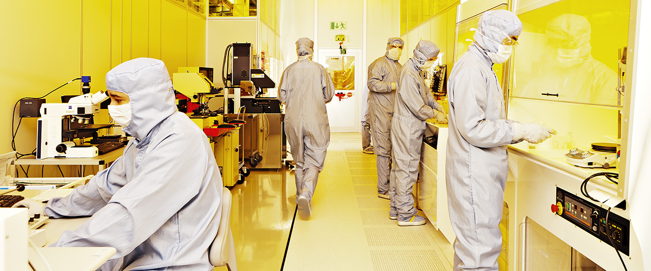
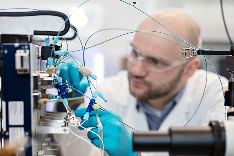
NTNU NanoLab is a 700 m2 cleanroom, providing general purpose equipment for the fabrication and characterisation of complex systems on the micro- and nanoscale. The cleanroom is an open-access user-operated facility, managed by a staff of nine full time engineers. As part of the “Norwegian Infrastructure for Micro-and Nanofabrication” (NorFab), NanoLab is open to researchers from across Norway, independent of their academic, institutional or company affiliation. International researchers may also use the facility.
The lab offers a wide range of thin-film deposition methods (evaporation, sputtering, chemical vapour deposition and atomic layer deposition), covering metals, insulators, semiconductors and piezo-electrics. It also offers a broad range of etching methods, including wet and dry etching chemical techniques and ion-milling. NanoLab provides extensive optical and e-beam lithographic equipment, enabling patterning of features down to 1 µm and 6 nm, respectively. Two maskless aligners are available within the lab for rapid optical lithography.
“Bottom-up” preparation of nanomaterials is catered for in a chemical clean-room equipped with fumehoods, laminar flow benches, a nitrogen glovebox, ovens, autoclaves, dip-coaters and a Langmuir Blodgett trough.
A wide range of characterisation equipment is available, including a scanning electrochemical microscope, a particle size analyser, absorption spectrometer, Atomic Force Microscopes (AFMs), a 3D profilometer, a contact angle measurement system, and three Scanning Electron Microscopes (SEMs). Compositional analysis may be carried out using X-ray photoelectron spectroscopy (XPS), Auger electron spectroscopy (AES) or µ-Raman spectroscopy. Focused ion beam (FIB) enables deposition, sputtering, serial tomography, TEM preparation and subsurface investigations.
Researchers wishing to access the facility may train to operate the equipment themselves or may hire the services of an operator. Users of the lab have the option of paying by-the-hour or paying for unlimited yearly access.
Contact: Dr. Peter Köllensperger
Norwegian Infrastructure for Micro and Nanofabrication (NorFab)
Norwegian Infrastructure for Micro and Nanofabrication (NorFab)
NorFab provides Norwegian and international researchers with access to state-of-the-art facilities for micro- and nano-fabrication, including thermal processes, thin film deposition, lithography, dry etching, characterisation, bonding and packaging, and chemical and biological methods. There are three geographical nodes located in Trondheim, Oslo and Horten:
NTNU NanoLab (Trondheim)
Please see above
Micro-System-Technology Lab (MST-Lab, University of South-Eastern Norway, Horten)
The MST-Lab at USN is a flexible cleanroom facility for MEMS processes on silicon wafers and other substrates, with an emphasis on bonding, packaging and Micro-System-Technology. The laboratory includes advanced tools for testing, dicing, pick and place, fine-pitch wire bonding and different flip-chip methods.
UiO MicroNanoLab (MiNaLab, University in Oslo)
UiO MiNaLab consists of one cleanroom floor and six laboratories with advanced synthesis, processing and analytical equipment, particularly suitable for semiconductors and materials science. The principal research areas are solar cell technology, semiconductor nanoscience, Micro-Optoelectronic Mechanical Systems (MOEMS), wide band-gap semiconductors and transparent conductive oxides.
SINTEF MicroNanoLab (MiNaLab, Oslo)
SINTEF MiNaLab is an industry-focused lab that performs R&D within microsystems and nanotechnology, including a complete Si processing line for 150 mm wafers. The focus is on silicon sensor research, prototyping and small-scale production. The lab is ISO 9001-2008 and ISO 14001-2004 certified, and is used by Norwegian and international industry for production of components.
![]() Please note, reciprocal arrangements exist between NanoLab, MST-Lab and UiO MiNaLab, entitling users with flat-rate access in one lab to equivalent access in the other labs at no additional charge.
Please note, reciprocal arrangements exist between NanoLab, MST-Lab and UiO MiNaLab, entitling users with flat-rate access in one lab to equivalent access in the other labs at no additional charge.
Learn more about NorFab here
Contacts:
TEM Gemini Centre / NORTEM node Trondheim
TEM Gemini Centre / NORTEM node Trondheim
The Norwegian Centre for Transmission Electron Microscopy (NORTEM) is a nationally coordinated initiative that makes state-of-the-art transmission electron microscopy (TEM) facilities available to Norwegian and international researchers. The Centre, which is co-located in Oslo and Trondheim, is a collaboration between NTNU, the University of Oslo and SINTEF. The Trondheim activity is run by the TEM Gemini Centre – a research team specialising in TEM from the Department of Physics, the Department of Materials Science and Engineering and SINTEF Industry. The Centre is part of the EU TEM network ESTEEM3.
The centre is equipped with three TEMs, extensive specimen preparation facilities, and a computer room for data processing. Each TEM has its own set of single and double tilt holders. Other options include cold-stage holders, heating holders, environmental cell holders, transfer holders, tomography holders and two tilt-rotation holders. Specimen preparation facilities include different types of dimplers, saws, ultrasonic cutters and other tools for the preparation of cross sectional specimens. The Centre has three precision ion-polishing systems, while an ultramicrotome is available for thinly slicing soft specimens. For applications requiring sample preparation on the nanoscale, there are two focused ion beam systems available at NTNU NanoLab.
The following TEMs are available within the Centre:
Jeol JEM-2100 LaB6 - this is the workhorse for routine TEM studies. It uses a heated lanthanum hexaboride (LaB6) filament as an electron source, and is configured for easy access and a broad user group; this is the instrument that new users are trained on. The set-up is optimized for conventional TEM techniques such as bright-field (BF) and dark-field (DF) TEM and selected area electron diffraction (SAED), but also EDX compositional analysis and HRTEM lattice imaging can be done.
Jeol JEM-2100F – this microscope is equipped with a field-emission gun (FEG) which – compared to conventional thermionic emitters such as tungsten and LaB6 – produces a narrower and more coherent electron beam with much higher current densities, resulting in better signal-to-noise ratio and spatial resolution for imaging and spectroscopy. The microscope is optimized for advanced materials studies, with a special focus on tomography and scanning precession electron diffraction (SPED), e.g. for phase and orientation mapping with high spatial resolution.
Jeol JEM-ARM200F – this is our most advanced TEM and is one of the best specified microscopes in Europe. Its use of a “cold” field emission gun ensures a sharper electron probe with a larger probe current, and thus permits atom-by-atom imaging and chemical analysis. The system has aberration correction for the probe and image forming lenses, and large efficient Energy-Dispersive X-ray (EDX) and Electron Energy Loss Spectroscopy (EELS) detectors for atomic scale spectroscopy.
Users wishing to access the TEM Gemini Centre may train to operate the equipment themselves or alternatively they can hire an operator through the TEM Gemini Centre. For more info see the TEM Gemini Centre webpage.
Contact: Prof. Randi Holmestad
NTNU Nanomechanical Lab
NTNU Nanomechanical Lab
 The Nanomechanical lab specialises in techniques for investigating the deformation and degradation of materials, interfacial mechanics and adhesion, and interactions between materials on the nanoscale. Detailed experimental investigations are supported by simulations involving ab-initio calculations, molecular dynamics and finite element methods. The lab is equipped with a variety of instruments for nanomechanical and nanotribological testing, including:
Two TI 950 TriboIndenters (Bruker Hysitron TI 950). The instruments allow Young’s modulus, hardness and fracture toughness to be measured by nanoidentation, while scratch resistance, critical delamination forces and friction coefficients can be quantified by scratch testing. In-situ scanning probe microscopy using the indenter tip provides surface topography information for hard and soft materials, and allows observation and quantification of material deformation, e.g. pile-up, wear volume, crack length and scratch morphology.
A dynamic tensiometer (Dataphysics DCAT 11) for the weight-based measurement of contact angle, surface tension, interfacial tension, and critical micelle formation concentration.
An environmental SEM (FEI Quanta FEG 650 ESEM ) for imaging wet or uncoated samples. The microscope is equipped with an electron backscatter diffraction (EBSD) detector for microstructural-crystallographic analysis, an in-situ picoindenter for nanomechanical testing, and an in-situ tensile module for tensile, and compression tests of specimens.
Users wishing to carry out measurements in the nanomechanical lab may train to operate the equipment themselves or collaborate with a research team member.
Websites: NanoMechanical lab and Multiscale Materials Science group
Contacts: Jianying He and Nuria Espallargas
Molecular Beam Epitaxy (MBE) lab
Molecular Beam Epitaxy (MBE) lab
 The MBE lab specialises in epitaxial growth (deposition) of III-V semiconductors in ultra high vacuum (UHV). The UHV condition allows evaporated materials to behave like molecular beams that can be easily interrupted by the use of shutters, permitting the fabrication of multi-layer structures with atomically sharp interfaces. The use of elemental sources whose deposition rates can be individually adjusted (by changing the source temperature) allows alloys such as AlxGa1-xAsySb1-y to be fabricated. Layers can be doped by co-deposition of a doping material, with a wide range of doping concentrations being possible. Growth of both thin-film structures and nanostructures, like nanowires and quantum dots, is possible. The lab usually stocks GaAs, GaSb, InAs, InP and Si as substrates.
The lab consists of 2 MBE systems:
Veeco Gen 930 MBE dedicated to arsenides, antimonides and dilute nitrides: Sources available: Ga x 2, In, Al, As, Sb and N plasma. Dopants: GaTe, Si and Be. Maximum sample size: 3” wafer. Holders for 2”, ¼ of 2” and 1x1 cm. Maximum substrate temperature 1200 °C as measured by themocouple (TC).
Veeco/Varian Gen II MBE dedicated to full nitrides (e.g. GaN): Sources available: Ga x 2, In, Al, N plasma (high growth rate) and possibly Sb. Dopants: Si and Mg. Maximum sample size: 3” wafer. Holders for 2”, ¼ of 2” and 1x1 cm. Maximum substrate temperature above 1200 °C as measured by TC, higher for small samples.
In addition, there is a CV-profiler in the lab that can be used to determine doping profiles in samples (GaAs, Si, p-type GaN, InAs, InP) by destructive etching (while measuring the capacitive response of the semiconductor-electrolyte interface).
Users can be trained to operate the MBE systems, but this is a lengthy process that is only suitable for long-term projects. For smaller projects, collaboration with a research team member is preferred. User operation is straightforward for the CV-profiler.
Contacts:
Atom Probe Tomography Laboratory (APTL)
Atom Probe Tomography Laboratory (APTL)
 Recently installed in the department of materials technology, the Cameca LEAP 5000 Atom Probe Tomography setup enables 3D imaging and chemical composition measurements to be carried out at the atomic scale. The atom probe forms part of the newly established Norwegian national centre for Minerals and Materials Characterisation (MiMaC) – a collaboration between NTNU, SINTEF and the Geological Survey of Norway that aims to establish a world class facility for the structural characterization and chemical analysis of minerals, metals and advanced nanomaterials.
In brief, Atom Probe Tomography works by taking a sample prepared in the form of a sharp needle shaped tip and subjecting it to a high DC bias to generate a large electric field at the sample tip, just below the threshold for atom evaporation. Further perturbation of the tip by a train of laser or voltage pulses is sufficient to trigger evaporation, causing individual ions to be emitted sequentially from the surface. By detecting their emission with a position-sensitive detector (PSD), it is possible to construct a three-dimensional image of the original sample, with the transit time from the sample to the PSD indicating the mass-to-charge ratio of each detected ion.
A wide range of materials may be analysed by Atom Probe Tomography, including metals, alloys, intermetallics, semiconductors, oxides and thin films. Key applications include: chemical analysis of nanoparticles; nanoscale compositional analysis and 3D imaging of grain boundaries in metals and alloys; investigation of interfaces in multilayer structures; analysis of phase separation in complex media; and spatial mapping of trace elements or dopants.
An accessible discussion of atom probe tomography (materialstoday - ScienceDirect)
The Atom Probe was installed in December 2018, and is expected to be fully operational by summer 2019. Users wishing to access the Atom Probe will have the option to train as users, hire an operator through MiMaC, or collaborate with a member of the Atom Probe research team.
For more infromation and contacts, see the Atom Probe Tomography web page.
The X-ray Physics Laboratory
The X-ray Physics Laboratory

The facility includes a Nikon 3D scanner for imaging with resolution down to about 5 micrometres, which is extensively used by both internal and external users. Adequate sample environments are available for in-situ thermal and mechanical loading. The lab further contains a unique X-radiography facility for dynamic imaging of evolving microstructures during solidification in alloy samples. A custom-built setup is available for small-angle X-ray scattering (SAXS) and wide-angle X-ray scattering (WAXS) analysis – built with a focus on flexibility for physics experiments. Finally, a phase-contrast computed tomography (CT) instrument based on a partially coherent nano-focus source is currently under construction and will be commissioned early 2022, aiming for sub-micron resolution and improved contrast for studies of soft and organic materials.
CONTACTS: Dag W. Breiby, Basab Chattopadhyay, and Ragnvald Mathiesen
Norwegian national centre for Minerals and Materials Characterisation (MiMaC)
Norwegian national centre for Minerals and Materials Characterisation (MiMaC)
 MiMaC is a new a collaboration between NTNU, SINTEF and the Geological Survey of Norway that aims to establish a world class facility for the structural characterisation and chemical analysis of minerals, metals and advanced nanomaterials. The Centre will provide structural characterisation facilities from the atomic scale through to the microscale, and will enable sensitive compositional analysis down to the parts-per-billion level. The instruments available within the centre include the following:
Atom Probe Microscope (Cameca LEAP 5000) for atomic scale compositional analysis and tomography, see above.
Electron Probe Microanalyser (JEOL JXA-8530FPLUS) which provides compositional information by exciting a sample with an electron beam and using the spectral characteristics of the emitted x-ray photons to identify elemental species. Measurements may be carried out on the few-hundred-nanometre length-scale due to the use of a field emission gun as the electron source.
Field Emission Scanning Electron Microscope (Zeiss Sigma 300 VP) with an image resolution of ~ 1 nm. The microscope has a Variable Pressure (VP) secondary electron detector that compensates for charging effects by controlling the chamber pressure, leading to sharp images with high contrast. The microscope is also equipped with an electron backscatter diffraction (EBSD) detector for microstructural-crystallographic analysis and an energy dispersive x-ray (EDX) detector for high resolution compositional analysis.
Split stream laser ablation instrument (Cetac G2) with parallel mass spectrometry (MS) and tandem MS detection channels for simultaneous analyses of elemental and isotopic compositions in minerals and materials.
Laser ablation system (Cetac G2) with triple quadrupole Inductively Coupled Plasma mass spectrometer (Agilent 8900 ICP-QQQ-ICP-MS) for direct surface analysis of elements in solid samples.
Most instruments are expected to be fully operational by mid 2019. Researchers wishing to access specific instruments will have the option to train as users, hire an operator through MiMaC or collaborate with a member of the MiMaC research team.
Contact: Ida Westermann
Ugelstad Laboratory
Ugelstad Laboratory
 The Ugelstad Laboratory was established in 2002 in memory of Professor John Ugelstad, and provides a wide range of experimental techniques for colloid, polymer and surface chemistry. The Lab has a strong focus on complex interfaces (especially in relation to dispersion stability and multiphase flow), and addresses application areas such as crude oil production and processing, water treatment, and materials science. The Laboratory uses a wide range of techniques for investigating solid/liquid, liquid/liquid, gas/liquid and gas/solid interfaces. Listed below are some of the key methods available within the Lab that may be of interest to nano-researchers:
Tensiometry The Lab offers multiple methods for measuring dynamic and equilibrium surface tensions. The appropriate choice of method varies according to the type of information sought, but we are able measure interfacial tensions by ring tensiometry, spinning drop tensiometry, pendant drop tensiometry and maximum bubble pressure tensiometry.
Dispersion characterization and stability Drop size distributions and stability of dispersions can be measured using a Turbiscan Lab Expert instrument or by low-field Nuclear Magnetic Resonance (NMR) spectroscopy. Flow and structural properties of dispersions can be followed using a rheometer.
Thermal analysis Differential Scanning Calorimetry (DSC) is available for investigating glass transitions, melting, crystallization, asphaltene precipitation kinetics, and paraffin wax analysis. A Thermogravimetric Analyzer (TGA) with Differential Scanning Calorimeter provides simultaneous measurements of weight change and differential heat flow in samples; it may also be used to investigate thermal stability, film stability, oxidation processes, surfactant stability and asphaltene pyrolysis. Interactions between components and self-association of molecules can be studied using an Isothermal Calorimeter.
Particle and surface characterization We offer dynamic light scattering and laser diffraction for determining particle sizes in solution, and electrophoretic mobility measurements for studying the surface properties of the particles. A Quartz Crystal Microbalance with Dissipation Monitoring is available for monitoring molecular events in real-time, measuring the mass and thickness of molecular layers, and analysing the structural properties of molecular layers.
Optical and spectroscopy techniques We offer optical and fluorescence microscopes for imaging, and a combination of Fourier-Transform Mid Infrared, Fourier-Transform Near Infrared and UV-vis spectrophotometers for absorption measurements. A High-Resolution Raman Microscope instrument is available for carrying out Raman measurements in the UV, VIS or NIR, while a fluorimeter is available for steady-state absorption and emission spectroscopy as well as for fluorescence lifetime measurements by time-correlated single photon counting (TCSPC).
Chromatographic methods We offer instrumentation for high performance liquid chromatography, using UV- and RI-detection. A combined GC-MS instrument can give structural information about samples.
Universal Microfluidic Platforms We have designed several microfluidic setups to look at the coalescence of multiphase systems and to study multiphase flow in porous structures.
Miscellaneous The following additional items are available in the Lab: a Karl Fisher Coulometer for water purity determination, a Critical Electric Field Emulsion Stability Cell for testing the stability of water-in-oil emulsions, and density and conductivity meters.
Researchers wishing to access the facility should request a research collaboration with Ugelstad Laboratory.
Website: Ugelstad Laboratory - Colloid and Polymer Chemistry
Contacts: Gisle Øye or Jens Norrman
Other useful infrastructures
There are a number of other infrastructures within NTNU and Trondheim which, while not being directly related to nanoscience and nanotechnology, may be of use to researchers.
Mechanical Engineering workshop, NV
Mechanical Engineering workshop, NV
Staffed by a team of nine technicians and engineers, the fine mechanical engineering workshop designs, fabricates and repairs scientific and technical instruments. In consultation with researchers, the workshop can design instruments on request, modify or repair existing instruments, and design and make components. The workshop is equipped with a range of modern machinery for milling, turning, drilling, welding and soldering equipment, and can handle a broad range of systems, including vacuum, pressure, x-ray and optical equipment.
Website: https://www.ntnu.no/nv/ansatte/finmek
Contact: Øystein Hagemo
Glass Blowing workshop
Glass Blowing workshop
The workshop designs, makes and repairs a wide range of glassware for research and teaching. The workshop is able to process various types of glass, ceramic materials and precious metals, and has particular expertise at working with quartz.
Website: https://www.ntnu.no/nv/om/glassverksted
Contact: Astrid Salvesen
NTNU Elprolab
NTNU Elprolab
The electronics and prototype lab offers a fast and convenient onsite facility for fabricating single- and double-sided PCB’s, with a typical turnaround of less than one week. Further information about the PCB’s that can be made may be found here:
Website: https://i.ntnu.no/wiki/-/wiki/Norsk/Elektronikk+og+prototypelaboratoriet
Contact: elprolab@ies.ntnu.no
Make NTNU
Make NTNU
MAKE NTNU is a voluntary student organization that works for a better environment for project development, both in private and educational contexts, for all students at NTNU. Our vision is an engaging and inclusive creative environment, where everyone with creative ideas will have the opportunity to realize their projects. We therefore run the Makerspace, known as Makerverkstedet, where a wide range of equipment like 3D printers, sewing machines, soldering equipment, etc. is at your disposal. The workshop is open and accessible to everyone at all times, where only the 3D printers require a course to use.
Hackerspace NTNU
Hackerspace NTNU
Hackerspace NTNU is a student-driven organization open to all students regardless of the field of study. With us you will find new technology at your disposal, including drones, 3D printers and Virtual Reality equipment. Whether you want to get an LED lamp to blink or make a 3D model of Trondheim, the members of Hackerspace can offer varied and good expertise and help you with that. If you are wondering about something, have a project you want help with, or just want to chat off, we warmly welcome you at our workshop and slack channel.
Website: https://www.hackerspace-ntnu.no/about/
Contact: hackerspace-styret@idi.ntnu.no
IoT Protolab (Wireless Trondheim)
IoT Protolab (Wireless Trondheim)
The IoT Protolab is a modern open electronics laboratory where innovative people can come together to exchange and explore new ideas, technologies and inventions.
Our laboratory is equipped with a variety of tools, instruments and talented members that can help you realize your ideas faster, cheaper and better. Our current focus area is rapid prototyping of applications related to Internet of Things (IoT) and wireless technology. The laboratory is open to students and employees from NTNU, members of FAKTRY and other interested parties. Key facilities Include 3D printers, a PCB printer, and a semi-automatic pick and place machine for assembling prototypes.
Contact: Thomas Ulleberg